关于 AMD K6
AMD K6 于 1997 年 4 月推出。其 RISC 架构最初是在 NexGen 开发的,并在收购 NexGen 后被 AMD 改用于他们的项目。K6 是为了与 Intel Pentium MMX 和 Pentium II 竞争。事实上,K6 是第一个被认真对待的竞争对手,即使它在 FPU 密集型程序中无法完全跟上英特尔的 MMX 处理器。
新的 K6 微架构的优点:
- 一个快速整数单元和一个非常短的流水线
- 一个智能的两级分支预测单元
- 一个相对较大的翻译后备缓冲区
K6 提供 166 至 300 MHz 的处理器时钟和 66 MHz 的 FSB 。
AMD 的 K6-2 是 K6 的升级版,于 1998 年 5 月末在商店有售。为了能够与 Intel 的 Pentium II 抗衡,AMD 的 K6-2 被赋予了新开发的 3DNow!实现的指令集。即使这不能完全胜过 MMX 指令集,但它在加速 3D 应用程序方面是一个巨大的进步。
K6-2 型号提供 200 至 550 MHz的处理器时钟和从 66 至 100 MHz 不同的 FSB。只有带有 Super 7 插槽的主板才能支持这些处理器。
AMD 的 K6-III 处理器是 K6 系列的最后一个开发阶段,因此也是所有 Socket 7 处理器中速度最快的。这些处理器从 1999 年 2 月开始在商店里出售。与 K6-2 相比,K6-III 最重要的创新是集成在 CPU 上的排他连接的 L2 缓存,大小为 256 KB,可在全处理器时钟下工作。之前的型号 K6 和 K6-2 仍然必须在主板上使用明显较慢的二级缓存。
K6-2+ 基于 K6-III,在 CPU 中集成了 128 KB L2 缓存,与 K6-III+ 一样,采用 0.18 µm 工艺制造。这使得它可以在比 K6-2 和 K6-III 处理器更低的电压下运行。
K6-2+ 和 K6-III+ 处理器作为嵌入式和移动处理器提供,但也非常受“超频者”的欢迎。由于台式机机箱中的良好冷却选项,曾有人将 K6-III+/450 超频至 600 MHz。
K6 系列于 1999 年 6 月被新的旗舰产品 Athlon 与 K7 微架构取代。
Introduction
K6
After AMD’s plans with the K5 turned into a debacle, AMD again claimed that they had the solution to make them more than just discount alternatives to Intel: A chip with the power of a Pentium Pro, with MMX support and intended to fit into a standard socket 7. AMD delivered its much anticipated K6 chip in April of 1997, beating Intel’s Pentium II to the market by a month.
AMD showed their commitment to establishing themselves in the market when they purchased NexGen in 1996 and with it, the design for the Nx686 processor. NexGen had been intending to market this chip in its own socket, but AMD changed the design to fit the standard socket 7, added MMX support, and renamed it the K6. Despite the name implying a design evolving from the K5, it is in fact a totally different design that was created by the NexGen team and adapted after the AMD purchase.
The K6 was originally launched running at speeds of 166 and 200 MHz in April 1997. It was followed by a 233 MHz version later in the summer of 1997. The release of the 266 MHz version of this chip was not until spring 1998 when AMD were able to move to the 0.25 micron manufacturing process. The final iteration of the K6 design was released in May 1998 running at 300 MHz and continued with the K6-2.
Initially, the AMD K6 processors used Pentium II Rating (PR2) to designate their speed. The PR2 rating was dropped because the rated frequency of the processor was the same as the real frequency. This item was made in the month the K6 was released (week 17/1997 = April 21st - 27th, 1997) and has the initial PR2 marking.
K6-2
The K6-2 was a significant improvement over the K6. It built upon the K6’s processing core, with the addition of 21 new instructions called “3D Now!”. These are SIMD (Single Instruction Multiple Data) instructions designed to enhance the 3D geometry capability of the chip’s floating point unit. This allowed the K6-2 to overcome the handicap of the slow (relative to Intel) CPU which the K6 owned.
The K6-2 also saw the introduction of a 100 MHz front side bus. This was only available to owners of new Super Socket 7 motherboards which also included features such as AGP. All of these features helped to give the K6-2 performance fast enough to be a credible challenger to the dominant Pentium II. Performance of the two chips was broadly similar: the K6-2 tending to be faster for general-purpose computing, the Intel part clearly superior at floating-point tasks. The K6-2 was a very successful chip and provided AMD with the marketing base and the financial stability it would need to introduce the Athlon.
The K6-2 was originally manufactured in speeds of 266 & 300 MHz in May 1998. The 300 MHz chip saw the introduction of the 100 MHz bus over the conventional 66 MHz bus used by the 266 MHz chip. August 1998 a 333 MHz version on a 95 MHz bus has been released and was quickly followed by a 350 MHz version on the 100 MHz bus. November 1998 saw the release of the 366, 380 and 400 MHz versions of the chip. This has been followed by the release of a 450 MHz K6-2 in February 1999 and the 500 MHz version in August 1999.
K6-III
The K6-III was the last and fastest of all Socket 7 processors. It achieved the distinction of being the fastest x86 processor on the market on release, and remained highly competitive for a considerable time afterwards.
In conception, the design was simple: it was a K6-2 with an additional L2 cache. The original K6-2 had a 64 KB primary cache and a much larger amount of motherboard-mounted cache (usually 512 KB or 1 MB but varying depending on the choice of main board). In contrast the competing Intel parts used 32 KB of L1 cache and either 128 KB of full-speed secondary cache integrated into the CPU itself (Celeron) or 512 KB of half-speed cache mounted on a processor daughter board (Pentium II, Pentium III). The K6-III, however, used both methods: it had 64 KB primary cache, a massive 256 KB on-chip, full-speed secondary cache (similar to the Celeron’s but twice the size), and the variable size motherboard mounted cache on the Socket 7 main board became a tertiary level.
In execution, however, the design was not simple: with 21.4 million transistors, it was a very large chip to manufacture with early 1999 technology, and the K6 core design did not scale well past 500 MHz. Nevertheless, the K6-III 400 sold well, and the K6-III 450 was clearly the fastest x86 chip on the market on introduction, comfortably outperforming AMD’s K6-2s and Intel’s Pentium IIs.
K6-2+
The K6-2+ is a revised version of the K6-III. Essentially, the K6-2+ is a K6-III with a 128 KB L2 cache made on a new 180nm production process. It was also the first processors to be available with the PowerNow! power saving technology. Essentially, the power savings were achieved with a combination of frequency (through adjusting multipliers) and voltage reduction.
我的收藏
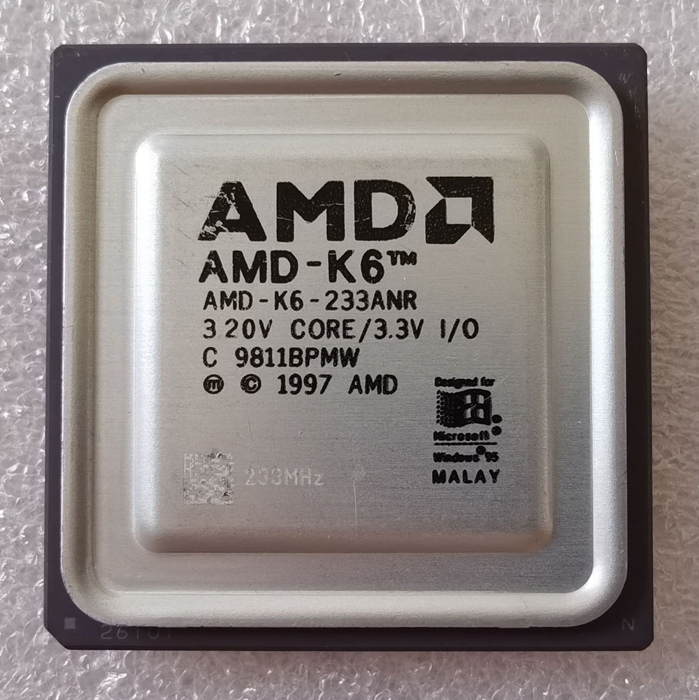
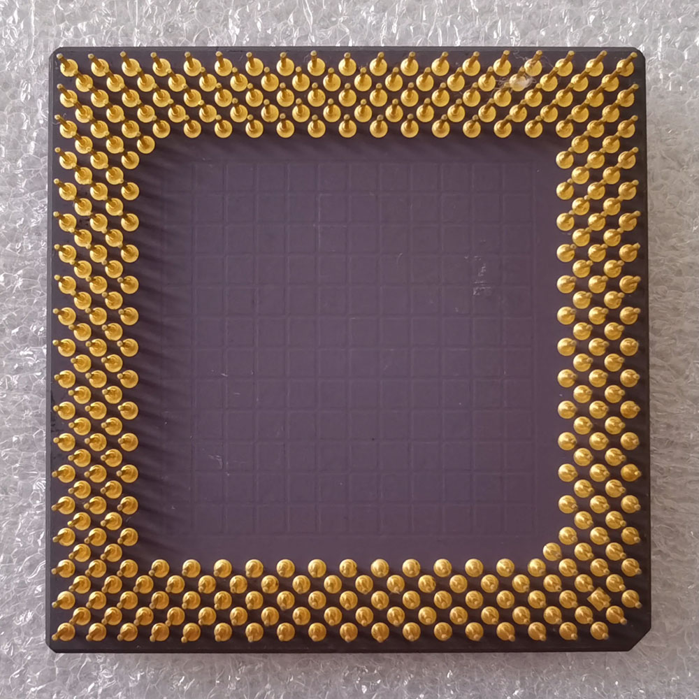
AMD-K6-233ANR
| 参数 | 数值 |
|---|---|
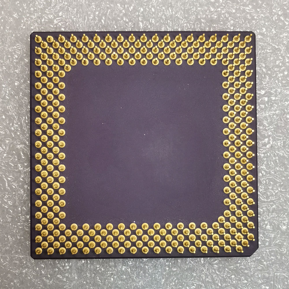
| CPU 类型 | 321-Pin CPGA |
| 核心 | K6 (Model 6) |
| Socket | 7 |
| 主频 | 233 MHz |
| 外频 | 66 MHz |
| 倍频 | x 3.5 |
| 总线宽度 | 64/32 Bit |
| 一级缓存 | 64 KB (32/32) |
| 晶体管 | 8,800,000 |
| 技术 | CMOS 0.35 µm |
| 生产日期 | 11/1998 |
  A = CPGA 设计
  N = 3.2 Volt Core (3.3 Volt I/O)
  Q = max. 70°C
  黑色标签
  带有 OR 代码和 CPU 时钟
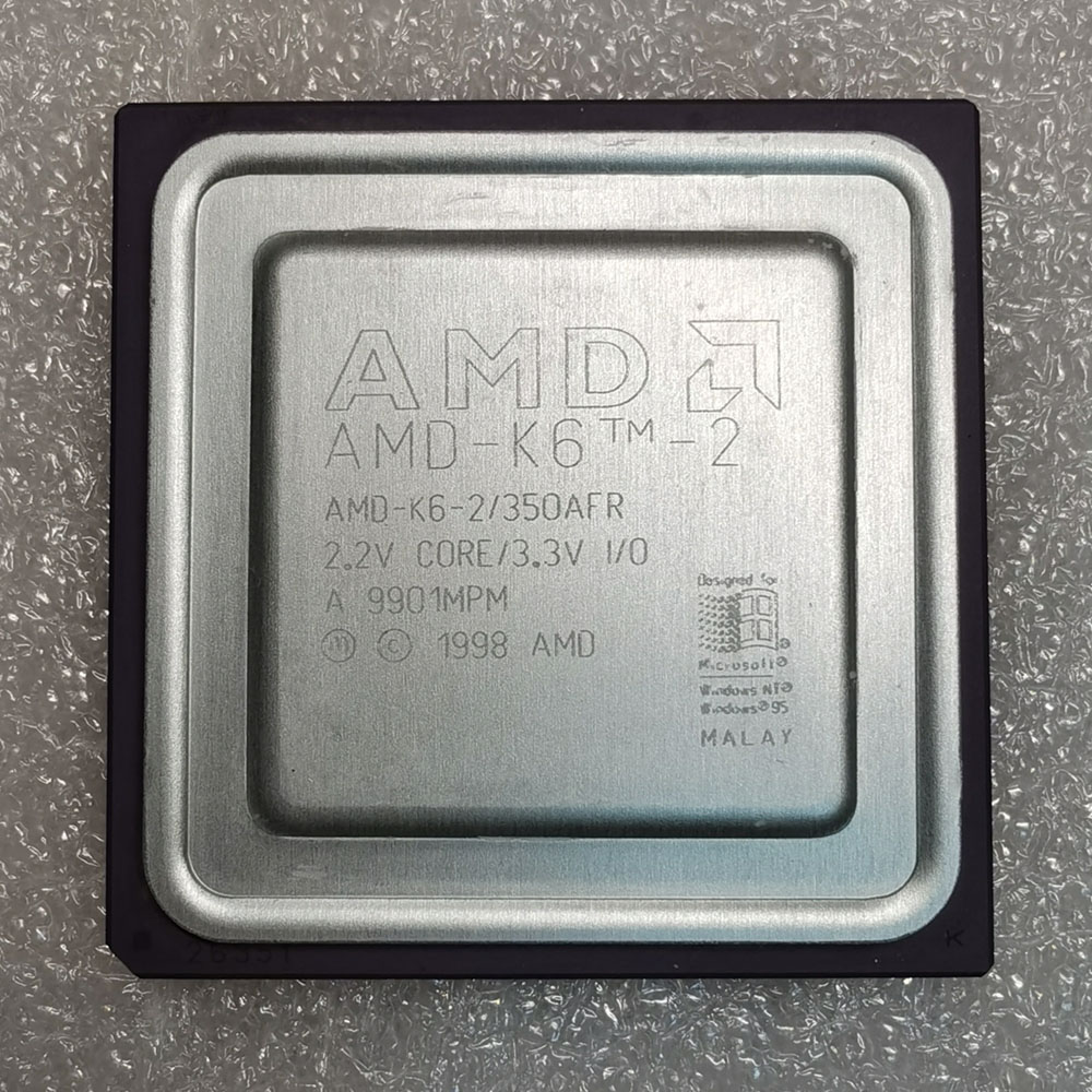
AMD-K6-2/350AFR
| 参数 | 数值 |
|---|---|
| CPU 类型 | 321-Pin CPGA |
| 核心 | Chomper |
| Socket | Super 7 |
| 主频 | 350 MHz |
| 外频 | 100 MHz |
| 倍频 | x 3.5 |
| 总线宽度 | 64/32 Bit |
| 一级缓存 | 64 KB (32/32) |
| 晶体管 | 9,300,000 |
| 技术 | CMOS 0.25 µm |
| 生产日期 | 01/1999 |
  A = CPGA 设计
  F = 2.2 Volt Core (3.3 Volt I/O)
  R = max. 70°C
  也作为嵌入式 CPU 出售
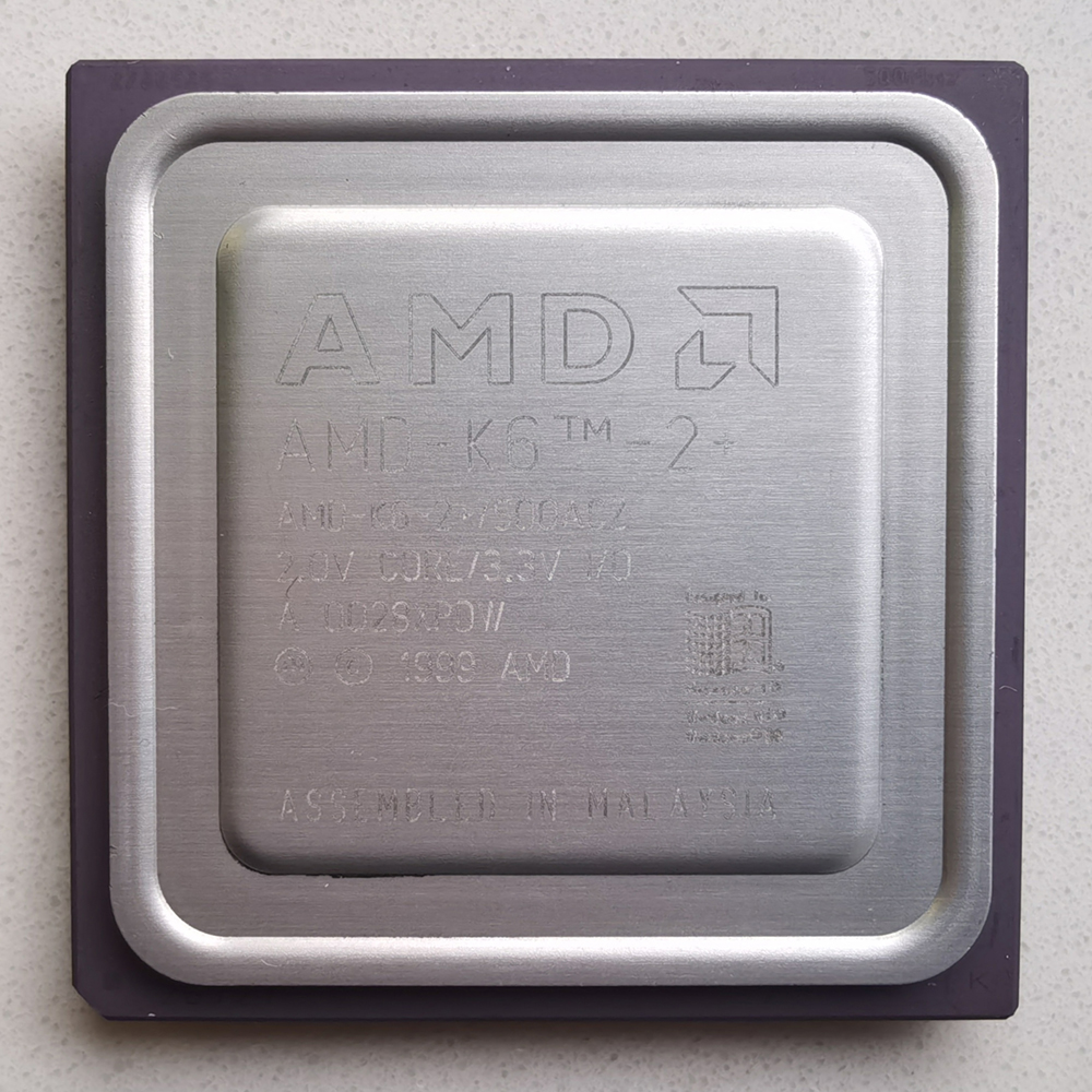
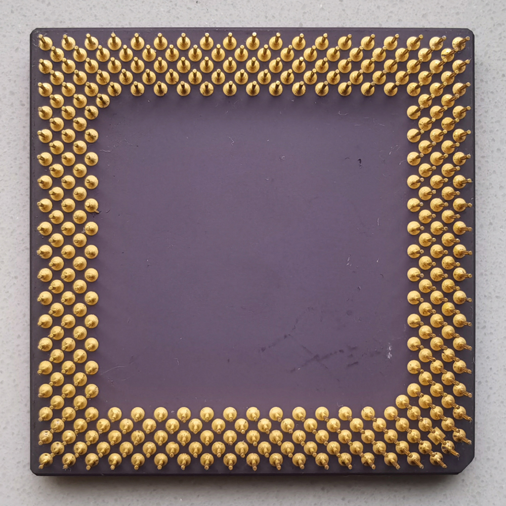
AMD-K6-2+/500ACZ
| 参数 | 数值 |
|---|---|
| CPU 类型 | 321-Pin CPGA |
| 核心 | |
| Socket | Super 7 |
| 主频 | 500 MHz |
| 外频 | 100 MHz |
| 倍频 | x 5 |
| 总线宽度 | 64/32 Bit |
| 一级缓存 | 64 KB (32/32) |
| 二级缓存 | 128 KB |
| 晶体管 | |
| 技术 | CMOS 0.18 µm |
| 生产日期 | 28/2000 |
  A = CPGA 设计
  C = 2.0 Volt Core (3.3 Volt I/O)
  Z = max. 85°C